
Product Overview
Selection Positioning
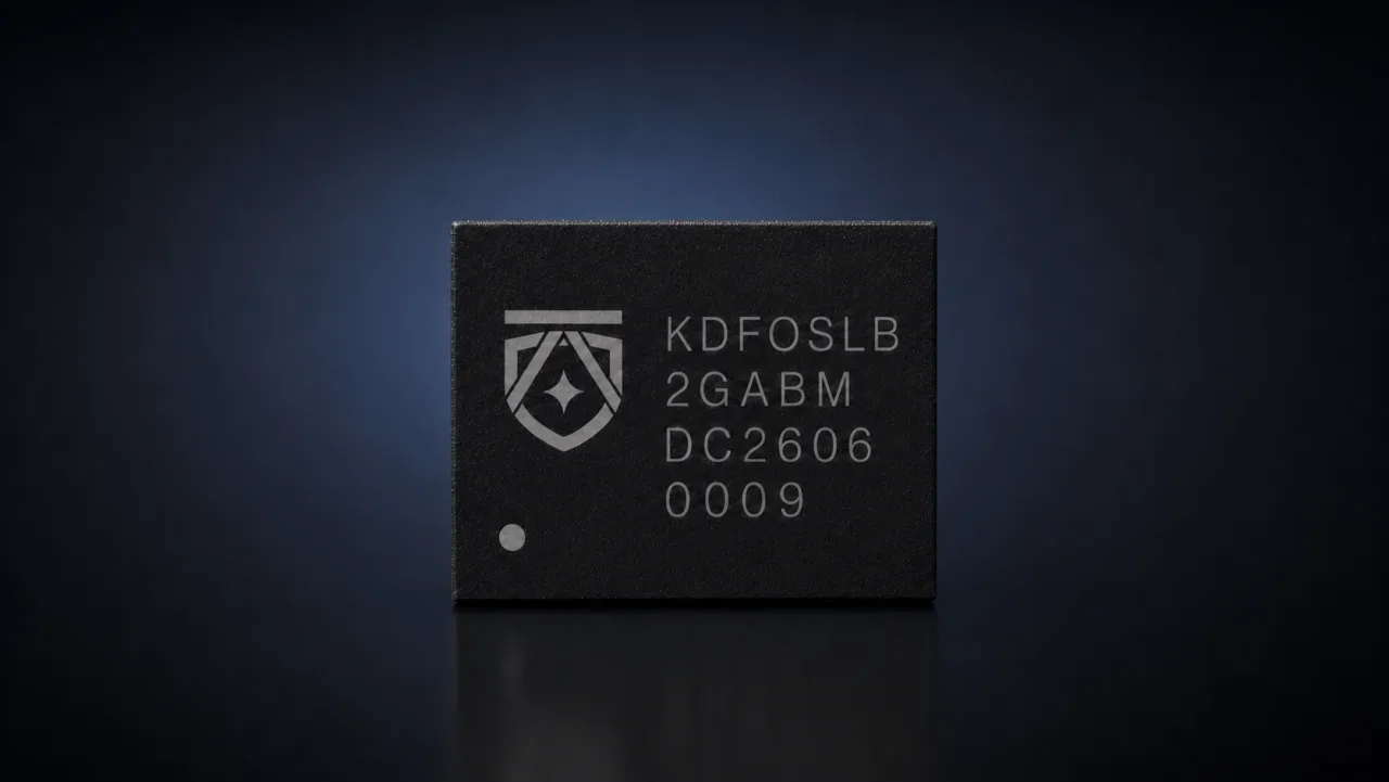
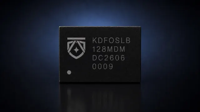
KDFOSLB2GABM is a 2Gb SPI NOR Flash with 1.8V supply for boot code, FPGA configuration, parameter storage and firmware update paths.
Capacity Conversion256MByte
Interface ModesStandard SPI / Quad SPI / DTR / QPI, 3-byte or 4-byte addressing
Read Performance133MHz fast read; Quad/QPI up to about 532Mbits/s; DTR Quad up to about 672Mbits/s
Power / Consumption1.65V to 2.0V single supply; typical standby about 40uA and power-down about 8uA
Package InformationPBGA-24, approx. 6mm x 8mm
Compatibility ReferenceMT25QU02G
Key Features
- 4KByte sectors, 32/64KByte blocks and 256Byte page programming; XIP and continuous wrap read support reduce boot and instruction-fetch latency.
- Hardware/software write protection, block protection, OTP security register options and unique ID support secure configuration flows.
- At least 100k program/erase cycles and typical 20-year data retention support long-lifecycle embedded systems.
Typical Applications
- Processor boot Flash, FPGA configuration Flash, board parameter area, firmware image and calibration/log storage.
- Replacement review should confirm voltage version, package pinout, address mode, boot-ROM read commands and erase/program timing.
Design-in Notes
- Confirm host processor, FPGA or SoC interface support, voltage rails and package footprint constraints.
- Before sample design-in, share schematic, PCB stack-up, clock/reset design, power sequencing and replacement part information.
- For replacement projects, provide the original part number, operating temperature, speed grade, package constraints and lifecycle requirement.
Selection Support
For platform compatibility, replacement review, temperature range, package constraints or document status, please submit the target platform, expected volume and project phase. Kangda sales and FAE teams can follow up with that context.
 KDFOSLB1GABM
 KDFOSLB256ME
 KDFOSV256MF
 KDFOSLB128MD